Field-programmable gate array
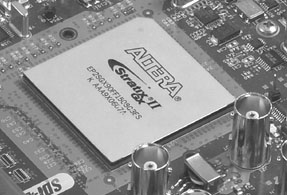
A field-programmable gate array (often shortened to FPGA) is an electronic component used to build reconfigurable digital circuits. That means that an FPGA is different from a logic gate, because a logic gate has a fixed function. In contrast an FPGA has an undefined function at the time of manufacture. Before the FPGA can be used in a circuit it must be programmed, that is, reconfigured.
FPGAs are integrated circuits in the category of programmable logic devices or PLDs. FPGAs are the highest performance, most flexible and also the most expensive of the PLD types. A drawback of FPGAs compared to other PLDs is that they do not remember their design when the power is removed. An FPGA therefore needs a separate configuration memory chip that holds the FPGA design. When the power is given back to the FPGA a fixed part of the FPGA reads the configuration from the configuration memory chip. After the FPGA is configured it will be able to do the function it was given by the design.
An FPGA is different from a microprocessor or microcontroller. An FPGA in its basic form is not able to run software. Only when the FPGA is given a configuration that contains a processor-architecture it has the ability to run software.
FPGA manufacturers provide engineering software for Windows and sometimes also Linux, to develop designs for FPGAs. The design is commonly written in human readable computer files called a hardware description language (HDL). The most popular hardware description languages are VHDL and Verilog. Hardware description languages are strongly comparable to programming languages. But the intention of HDLs is to design digital logic circuits while programming languages design software.
The FPGA engineering software has to translate the abstract HDL code into the logic elements available in the selected FPGA. That is called logic synthesis. Then a process of place and route is done to position the logic elements in the FPGA. The result is a bitfile that can be programmed into the FPGA or the configuration memory. This is usually done with a USB programmer connected to the JTAG port of the FPGA.
Because the FPGA is an integrated circuit, an FPGA manufacturer can decide to add other commonly used integrated circuit components. These fixed parts are called cores. These are for example Ethernet controllers or even a complete processor-architecture. For different market segments such as defense, medical, communications and robotics the FPGA manufacturer tries to add the most valuable set of these additional cores.
Internal structure
FPGAs are generally built upon programmable logic elements and programmable interconnects. One building block of logic elements is a programmable lookup table (LUT). A LUT can be programmed to output any value given input values. In this way, a LUT can be programmed to be any type of logic with the same number of inputs and outputs. For example, a 2-input, 1-output LUT can be programmed to emulate the logic of a 2-input AND, OR, NAND, NOR, XOR, etc. The output of this LUT can be either saved using a register or connected to the input of other LUTs. Using a programmable mux, the FPGA can be programmed to choose the registered or non-registered output. This combination of a LUT, a register, and a mux is the general structure of a logic element.
To connect these logic elements together, pass transistors are used. The transistor can be programmed to either connect a signal or not, thereby giving the FPGA the ability to very specifically connect logic elements together. For example, if the output of one logic elements will feed the input of another, the pass transistor can be programmed to connect these two wires together and match the specified logic. Between the logic elements and the pass transistors, a compiler can take a hardware description from an HDL, create the logic for the logic elements, and connect them together using the pass transistors.
Field-programmable Gate Array Media
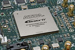
A Stratix IV FPGA from Altera
Simplified example illustration of a logic cell (LUT – lookup table, FA – full adder, DFF – D-type flip-flop)
A Xilinx Zynq-7000 all-programmable system on a chip


