Scanning tunneling microscope

Scanning tunneling microscopy (STM) is a way to view the shape of tiny objects. It can make pictures of atoms on a surface and move the atoms to different places. It was invented by Gerd Binnig and Heinrich Rohrer in 1981 at IBM, in Zürich. In 1986 they won the Nobel Prize in Physics for inventing it.[1]
How it works
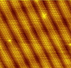
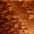
The STM is called a microscope because it makes pictures of tiny objects. But it is different -- it doesn't have anything to look into with our eyes. It is similar to feeling the shape of objects on a table in a dark room: you can draw a picture of the shape even though you did not seen it with your eyes. The STM does this for very tiny objects. It works by scanning a sharp metal needle back and forth across a surface, and uses electric current instead of force to sense the shape. When the tip of sharp metal needle is brought very close to the surface of a thing being studied, a voltage between the two causes electrons to flow through the space between them. The electrons cross this space by a process called quantum tunneling, which gives the STM its name. This tiny current of electrons flows when the tip is almost touching the surface. The current changes as the probe moves along the surface. This change is recorded by a computer, which makes it into a picture that we can see.
The surface and the tip must conduct electrons, so they must be made of a metal or semiconductor. A related kind of microscope senses the force instead of the electric current. This kind of microscope is called an atomic force microscope.
STM is a hard thing to do, because it needs a very clean surface and a very sharp needle tip. The STM usually works in a vacuum to keep the air molecules from disturbing the surface, but it can also work in air or water.[2]
Ways it can make a picture
First, the tip is brought very close to the surface of thing being studied. This distance is about half of a nanometer. Then the tip is moved very carefully back and forth across the surface. The electrical current is measured while the tip is moved back and forth (constant height method). The STM can also work by adjusting the tip so the tunnel current stays the same (constant current method).[2] Using the constant-height method is faster. Using constant-current method helps avoid bumping the tip into things on the surface, so it can study things that are rougher.
Moving atoms
The STM can move an atom (or a molecule) to a new place on the surface. To move an atom, the tip is moved so it touches the atom. Then the tip pulls or pushes the atom to a new place. Moving atoms allows scientists to arrange them into tiny objects, so they can test their properties and try out new ideas.
Parts of the STM
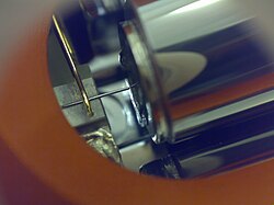
The parts of an STM are: scanning tip, something that moves the tip, something that stops it from vibrating, and a computer that controls the tip and makes the picture.

Scanning Tunneling Microscope Media
Scanning tunneling microscope operating principle
A 1986 STM from the collection of Musée d'histoire des sciences de la Ville de Genève
A large STM setup at the London Centre for Nanotechnology
Related pages
References
Other websites
![]() Media related to Scanning tunneling microscope at Wikimedia Commons
Media related to Scanning tunneling microscope at Wikimedia Commons
- Scanning Electron Microscope is filming a STM Archived 2007-09-27 at the Wayback Machine (mpeg movie 3MB)
- Zooming into the Nanoworld Archived 2008-05-21 at the Wayback Machine (Animation with measured STM images)
- SPM - Scanning Probe Microscopy Website Archived 2008-04-10 at the Wayback Machine
- STM Gallery at Vienna University of technology
- Build a simple STM with a cost of materials less than $100.00 excluding oscilloscope Archived 2014-07-08 at the Wayback Machine
- Nanotimes Simulation engine download page Archived 2009-03-16 at the Wayback Machine
- Structure and Dynamics of Organic Nanostructures discovered by STM
- Metal organic coordination networks of oligopyridines and Cu on graphite investigated by STM
- Surface Alloys discovered by STM Archived 2008-09-08 at the Wayback Machine
Literature
- Tersoff, J.: Hamann, D. R.: Theory of the scanning tunneling microscope, Physical Review B 31, 1985, p. 805 - 813.
- Bardeen, J.: Tunnelling from a many-particle point of view, Physical Review Letters 6 (2), 1961, p. 57-59.
- Chen, C. J.: Origin of Atomic Resolution on Metal Surfaces in Scanning Tunneling Microscopy, Physical Review Letters 65 (4), 1990, p. 448-451
- G. Binnig, H. Rohrer, Ch. Gerber, and E. Weibel, Phys. Rev. Lett. 50, 120 - 123 (1983)
- G. Binnig, H. Rohrer, Ch. Gerber, and E. Weibel, Phys. Rev. Lett. 49, 57 - 61 (1982)
- G. Binnig, H. Rohrer, Ch. Gerber, and E. Weibel, Appl. Phys. Lett., Vol. 40, Issue 2, pp. 178-180 (1982)
- R. V. Lapshin, Feature-oriented scanning methodology for probe microscopy and nanotechnology, Nanotechnology, volume 15, issue 9, pages 1135-1151, 2004


