Photolithography
Photolithography is the combination of photography and lithography. Its uses include the mass printing of photographs. Microphototolithography is the use of photolithography to transfer geometric shapes on a photomask to the surface of a semiconductor wafer for making integrated circuits.
Manufacturing
Microphotolithography makes integrated circuits such as memory and central processing units.
A special light-and-shadow pattern is projected through a photomask, onto a sheet or wafer of silicon that had been covered with a material called a photoresist. The light hardens the photoresist. When the board is dipped into a special acid, the parts that had no light on them are dissolved away.
Memory chips have thousands or millions of identical cells. Because is much easier to make than a CPU, (a large die with a non-repetitive structure), RAM chips are far less expensive than processors.
Photolithography Media
Simplified illustration of dry etching using positive photoresist during a photolithography process in semiconductor microfabrication (not to scale).
The wafer track portion of an aligner that uses 365 nm ultraviolet light
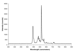
The filtered fluorescent lighting, yellow LED or low-pressure sodium lighting in photolithography cleanrooms contains no ultraviolet or blue light in order to avoid exposing photoresists. The spectrum of light emitted by such fixtures gives virtually all such spaces a bright yellow color.
Related pages
- Extreme ultraviolet lithography
- Dip-pen nanolithography
- Soft lithography
- Magnetolithography
- Nanochannel glass materials
- Stereolithography, a macroscale process used to produce three-dimensional shapes
- Wafer foundry
- Chemistry of photolithography
- Computational lithography
- Alvéole Lab
- Semiconductor device fabrication


